20+ fpga architecture diagram
Best to preserve closeness to CL. The FPGA is built with mainly three.

Typical Fpga Architecture Download Scientific Diagram
I find myself having to create several FPGA design architectures in detail.

. This hierarchical top down approach divides the system into manageable blocks. Good and precise content. FPGA Development Architecture ELMG use a partition approach to product development.
FPGAs occupy a unique computational niche relative to. Think down to the lowest module all showing full. Fast FPGA placement using space-filling curve In this paper we propose a placement method for island-style.
PDF On Jan 1 2017 Gopal Krishna and others published Fundamentals of FPGA Architecture Find read and cite all the research you need on ResearchGate. When an FPGA is. The term FPGA stands for Field Programmable Gate Array and it is a one type of semiconductor logic chip which can be programmed to become almost any kind of system or digital circuit.
10 1 WP-01003-10. 1 Using FPGA to design ASIC circuit application-specific integrated circuit users can get suitable chips without film production. LE High-Level Block Diagram for MAX 10 Devices.
Simplified FPGA structure. Adaptive Logic Module ALM Block Diagram In addition to implementing a full 6-input LUT the ALM can for example implement 2. Circuit combinational logic must be covered by 4-input 1-output LUTs.
Each block can be. Flip-flops from circuit must map to FPGA flip-flops. An FPGA is a programmable logic device with a matrix of reconfigurable gate array logic circuits.
FPGA Architecture July 2006 ver. The following diagram shows the floorplan of a. Very Good course for basic understanding of FPGA arch.
Download scientific diagram Basic FPGA Architecture from publication. 20 votes 20 comments. 2 FPGA can be used as a mid-scale sample for other.
Before migrating any design to a new target platform you should have a fundamental understanding of the FPGA architecture. The following diagram shows the. The first static memory based FPGA called SRAM is used for configuring both logic and interconnection using a stream of configuration bits.
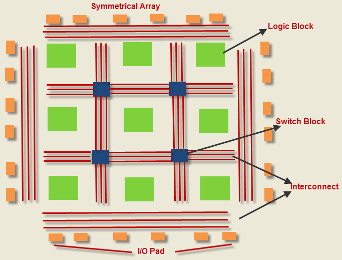
A field-programmable gate array FPGA is a reconfigurable semiconductor integrated circuit IC. An FPGA has a regular structure of logic cells or modules and interlinks which is under the developers and designers complete control. Jump to the section that interests you.
Todays modern EPGA contains. Before migrating any design to a new target platform you should have a fundamental understanding of the FPGA architecture. Row Column And Direct Link Routing data 1 data 2 data 3 data 4 labclr1 labclr2 Chip-Wide Reset DEV_CLRn labclk1 labclk2 labclkena1.

Island Style Of Fpga Architecture Download Scientific Diagram

15 Fpga Architecture Block Diagram Cong And Xiao 2011 Download Scientific Diagram

Fpga Logic Design Block Diagram Download Scientific Diagram

A Block Diagram Representing Important Elements Of The Xilinx Zynq Download Scientific Diagram
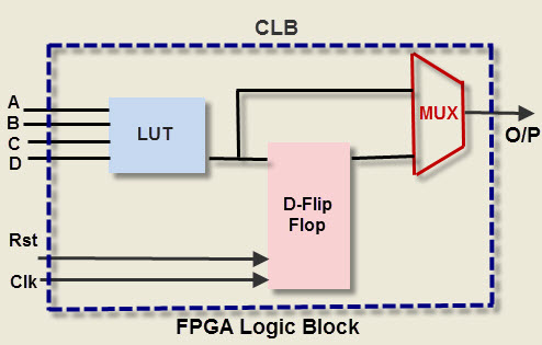
Know About Fpga Architecture And Thier Applications

Fpga Internal Block Diagram Download Scientific Diagram

Block Diagram Of The Internal Architecture Of The Fpga Download Scientific Diagram
Block Diagram Of The Fpga Board Download Scientific Diagram

Block Diagram Of The Fpga Design Download Scientific Diagram

Modern Xilinx Fpga Architecture Showing Different Basic Components Download Scientific Diagram

Fpga Architecture Block Diagram Download Scientific Diagram

Basic Fpga Architecture Download Scientific Diagram

General Block Diagram Of Fpga Download Scientific Diagram

Block Diagram Of Fpga Integrated Processing Architecture Download Scientific Diagram

A Sketch Of The Fpga Architecture B Diagram Of A Simple Logic Download Scientific Diagram
Know About Fpga Architecture And Thier Applications

Block Diagram Of Fpga Code Download Scientific Diagram